- Address
- 305-0044 茨城県つくば市並木1-1 [アクセス]
研究内容
- Keywords
ナノ材料・ナノバイオサイエンス 薄膜・表面界面物性
出版物2004年以降のNIMS所属における研究成果や出版物を表示しています。
所属学会
応用物理学会, 日本物理学会
電子・光機能材料研究センター
ヘテロエピタキシー新技術の開発
分子線エピタキシー,表面・界面構造解析,半導体積層構造,量子ドット
概要
革新的光・電子機能材料の実現に向けて、その礎となるエピタキシャル結晶成長技術の開発を進めている。分子線エピタキシー法に基づく高度な結晶成長技術と原子レベルでの表面・界面評価技術を駆使して、主に格子不整合系の半導体ヘテロ積層構造の作製と評価を行っている。
新規性・独創性
● 原子レベルでの表面構造の評価と制御に基づくヘテロエピタキシー過程の精緻な制御。
● (111)方位に特有な歪み緩和機構を利用することによって、低欠陥密度のIII-Vヘテロ積層構造を実現。
● 格子不整合に関する制約を受けにくいMoSe2やWSe2等の二次元層状物質を用いた多層ヘテロ積層構造を作製。
● 量子ドット形成過程のその場観察。
内容
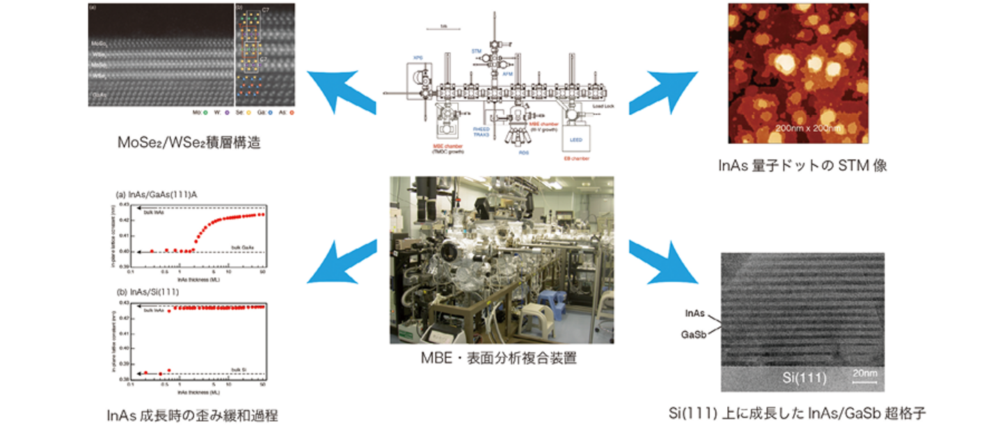
分子線エピタキシー装置と電子回折、電子分光、走査トンネル顕微鏡などの表面分析装置を備えた複合型装置を用いて、III-V族半導体および遷移金属ダイカルコゲナイドのヘテロ構造を作製・評価している。具体的には、次のとおり。
● (111)面に特有な歪み緩和機構を利用して、GaAs(111)AやSi(111)基板上に低欠陥のIII-Vヘテロ積層構造を作製する技術を開発し、赤外デバイスへの応用を進めている。
● 遷移金属ダイカルコゲナイドについては、格子不整合の影響を受けにくいという特徴を活かし、MoSe2やWSe2等の単層膜から構成される積層構造の作製技術を開発している。
● 量子ドットの高品質化に向け、NIMS独自技術である液滴エピタキシー法による量子ドット形成過程を原子レベルで評価し、成長メカニズムの解明を目指している。
まとめ
● 主にⅢ-Ⅴ族化合物半導体や遷移金属ダイカルコゲナイド等の材料を対象に、高度なエピタキシャル成長技術の開発を行い、それを駆使した新規ヘテロ構造の作製とその物性探索に関する研究を進めている。
● 原子レベルでの表面分析技術に基づく成長プロセスの精緻な制御方法を確立することにより、次世代光源や高感度センシングデバイス等の革新的な光・電子機能を有する半導体材料開発がより一層加速されると期待できる。