SAMURAI - NIMS Researchers Database

HOME > Profile > KAWAMOTO, Naoyuki
Research

Keywords

透過電子顕微鏡、局所導電性評価、電磁場評価

走査透過電子顕微鏡(STEM)を用いて、材料内部の熱輸送現象をナノスケールで計測・可視化する研究に取り組んでいます。独自に開発したSTEM熱解析顕微法(STAM)では、収束電子線を局所熱源、ナノ熱電対を温度センサーとして利用します。さらに、パルス電子線によって発生する温度波の振幅と位相を検出するパルスSTAM(p-STAM)の開発を進めています。これにより、熱拡散率、熱伝導の異方性、結晶粒界や異相界面における熱輸送特性を微細構造と対応させて評価します。半導体、熱電材料、セラミックス、複合材料などの熱輸送機構を解明し、高性能な熱制御材料・デバイスの設計に貢献することを目指しています。

researchPicture

PublicationsNIMS affiliated publications since 2004.

Books
Proceedings
Presentations
Misc

Society memberships

日本顕微鏡学会, 日本金属学会

Awards

  • 日本顕微鏡学会 第20回「奨励賞」(顕微法基礎部門) (2019)
  • Asian Association of Thermoelectrics 【The AAT Poster Prize 2018】 (2018)
  • 第62回 日本金属学会金属組織写真賞透過電子顕微鏡部門 「奨励賞」 (2012)
  • 第58回 日本金属学会論文賞「組織部門」 (2010)
  • 第56回 日本金属学会論文賞「まてりあ論文部門」 (2008)
  • 第55回 日本金属学会論文賞「工業材料部門」 (2007)
  • 青葉工学振興会 及川研究奨励賞 (2007)
  • 第54回 日本金属学会論文賞「若手講演論文」 (2006)

Funds

  • ナノスケール動的ステレオ熱輸送評価法の開発についての研究 (2024)
  • パルス電子線を用いた先端材料におけるナノ熱輸送評価についての研究 (2022)
  • 熱デバイス評価に向けたTEMによる高速ナノ熱輸送計測法の開発について の研究 (2020)
  • TEMを利用したナノスケール定常熱伝導評価手法の開発とその応用につい ての研究 (2014)
  • ナノチューブ探針による高精度TEM内局所電気計測手法の開発と微細配線評価への応用 (2011)
Center for Basic Research on Materials
Title

Development and Applications of a Nanoscale Thermal Transport Measurement Method in TEM Using a Pulsed Electron Beam

Keywords

Transmission electron microscopy, temperature measurement, thermal conductivity, pulsed electron beam, thermal wave, thermocouple, thermal diffusivity, in situ observation, TEM, STEM

Overview

My research focuses on elucidating the relationship between the microstructure of materials and their thermal transport properties at the nanoscale using transmission electron microscopy (TEM) and scanning transmission electron microscopy (STEM).

In particular, I am developing STEM-based Thermal Analytical Microscopy (STAM) and its pulsed-electron-beam variant, p-STAM. These techniques use a focused electron beam as a localized heat source and detect minute temperature variations propagating through a specimen with a nanoscale thermocouple. They are intended to visualize and quantify thermal transport across grain boundaries, heterointerfaces, defects, and nanostructures in direct correlation with the local microstructure—information that is difficult to obtain by conventional electron microscopy.

To date, I have validated the principles of these techniques using model materials such as sapphire and applied them to thermoelectric materials and ceramics. These studies have addressed thermal-conduction anisotropy, phonon scattering at grain boundaries, and interfacial thermal resistance. I am also developing instrumentation, specialized specimen holders, signal-detection systems, and analytical methods for in situ measurements of thermal transport phenomena inside an electron microscope.

By integrating structural and compositional characterization with nanoscale thermal measurements, my research aims to clarify thermal transport mechanisms in semiconductors, thermoelectric materials, ceramics, and other functional materials, and ultimately to provide design guidelines for advanced materials and devices with improved thermal-management performance.

Novelty and originality

A new concept for directly evaluating nanoscale thermal transport inside an electron microscope
Use of a focused electron beam as a localized heat source
Highly sensitive temperature measurement combining a nanoscale thermocouple with lock-in detection
Correlative analysis of microstructure and thermal transport in the same region
Potential expansion to in situ thermal transport analysis

Details

image

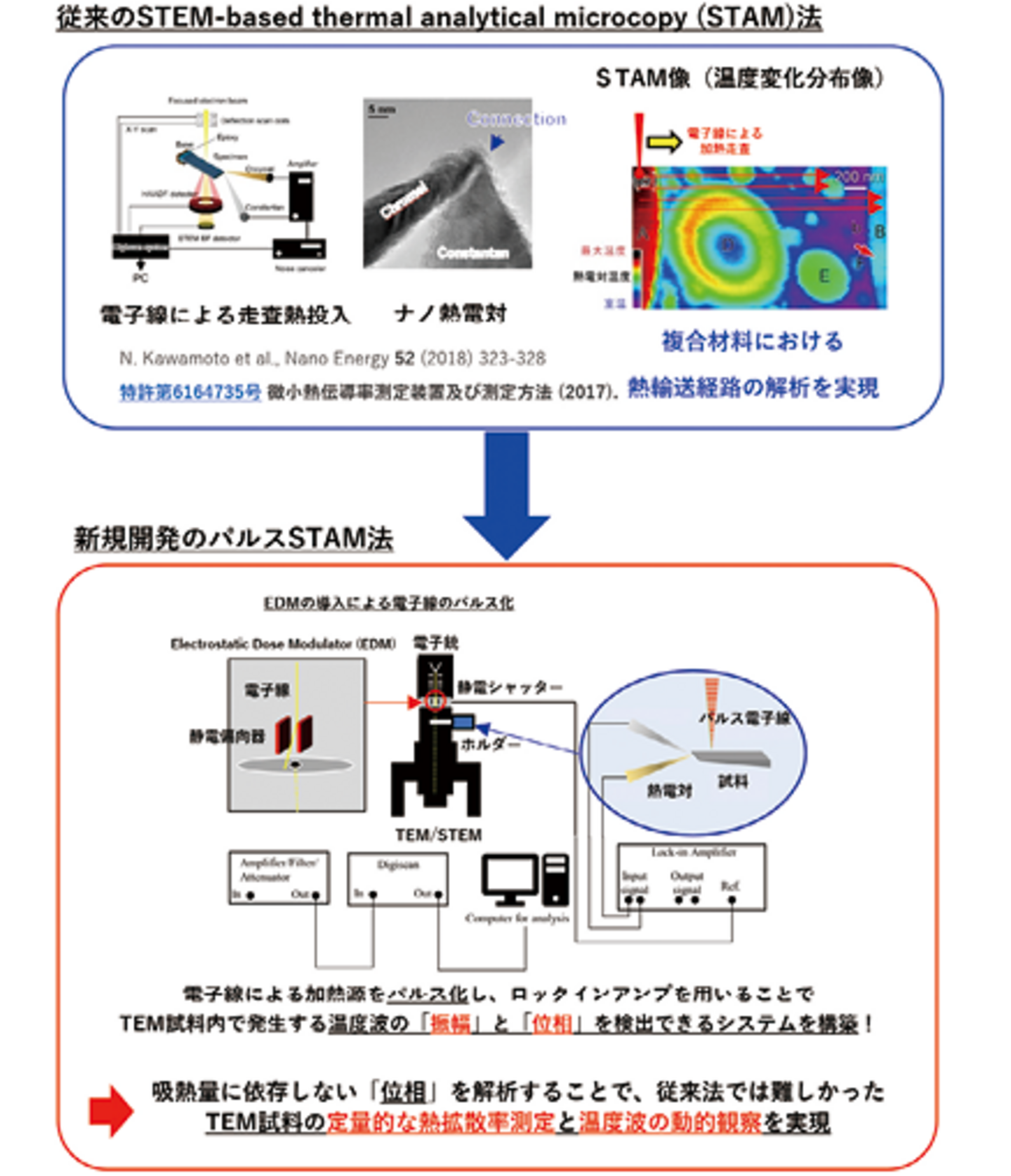
We have been developing an original technique, STEM-based Thermal Analytical Microscopy (STAM), for evaluating thermal transport properties at the nanoscale within a scanning transmission electron microscope. In conventional STAM, a focused electron beam is used as a localized heat source, while the resulting temperature change is detected using a specially developed nanoscale thermocouple placed in contact with the specimen. By scanning the electron-beam irradiation position and recording the corresponding thermocouple response, the spatial distribution of heat transport under steady-state conditions can be visualized as a STAM image.

For example, in heat-dissipation composites consisting of highly thermally conductive fillers embedded in a low-thermal-conductivity polymer matrix, STAM enables the analysis of heat-transport pathways through the fillers, polymer, and their interfaces in direct correlation with electron microscopy images. This approach therefore allows the effects of microstructure, composition, grain boundaries, and heterointerfaces on local thermal transport to be evaluated within the same specimen and observation area.

A limitation of conventional STAM is that the amount of heat deposited by electron-beam irradiation depends on factors such as specimen thickness, composition, density, and accelerating voltage. Quantitative analysis of thermal properties therefore requires careful consideration of the deposited heat input. To overcome this limitation, we are currently developing pulsed STAM, or p-STAM, in which an Electrostatic Dose Modulator equipped with an electrostatic shutter is installed in a transmission electron microscope to generate a pulsed electron beam at a controlled frequency. This enables periodic thermal waves to be produced within a TEM specimen.

In p-STAM, minute temperature variations generated by the pulsed electron beam are detected with a nanoscale thermocouple, and the amplitude and phase of the thermal waves are measured with high sensitivity using a lock-in amplifier. In particular, because the phase response is relatively insensitive to the absolute magnitude of the heat input, the thermal diffusivity of TEM specimens can be quantitatively evaluated while reducing the influence of uncertainties in electron-beam heating.

The measurement principle has been validated using model materials such as sapphire, and the technique is being applied to ceramics, thermoelectric materials, metals, and composite materials. Current studies focus on the evaluation of thermal diffusivity, crystallographic anisotropy in thermal transport, changes in heat conduction across grain boundaries, and thermal resistance at heterointerfaces. Another important feature of this method is its compatibility with HAADF-STEM imaging, electron diffraction, and elemental analysis, enabling direct correlation between local structure, composition, and thermal transport properties.

By integrating high-spatial-resolution structural and compositional characterization with quantitative thermal-property measurements based on thermal waves, this research aims to clarify nanoscale heat-transport mechanisms in semiconductors, thermoelectric materials, ceramics, and heat-dissipation composites, and ultimately to provide design guidelines for advanced thermal-management materials and devices.

Summary

We are developing an original thermal transport measurement technique, STEM-based Thermal Analytical Microscopy (STAM), which uses a focused electron beam as a localized heat source and a nanoscale thermocouple as a temperature sensor inside a scanning transmission electron microscope.We are also advancing pulsed STAM (p-STAM), in which the phase and amplitude of thermal waves generated by a pulsed electron beam are measured to quantitatively evaluate the thermal diffusivity and interfacial thermal resistance of TEM specimens.By integrating electron microscopy-based structural and compositional analysis with nanoscale thermal measurements, we aim to elucidate heat-transport mechanisms in semiconductors, thermoelectric materials, ceramics, and composite materials.

この機能は所内限定です。
この機能は所内限定です。

▲ Go to the top of this page