マテリアル基盤研究センター
Novel microscopy techniques for advanced characterization
Electric field mapping, Nanoscale temperature distribution, Thermal vibration mode imaging
概要
Our aim is to extend the range of information that can be obtained by transmission electron microscopy (TEM) by developing new analysis methods. By combining these new techniques with the already impressive capabilities of modern TEMs, we can measure material properties which are not accessible by any other methods. This furthers our understanding of the advanced materials investigated and provides feedback towards improving their performance.
新規性・独創性
• Atomic-resolution measurement of the distribution of electric fields around defects in 2-D materials
• Direct observation of the thermal vibration modes of individual nanowires
• Nanometer-scale temperature mapping of in-situ Joule-heated carbon nanotubes
内容

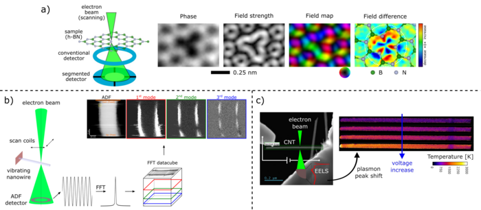
(a) By introducing new hardware and custom-developed software, we were able to build a multi-dimension data acquisition system which allows characterizing the electrostatic properties of materials. (b) With the addition of a high-speed data acquisition interface, we were able to acquire signals in the MHz range and thus measure the vibration properties of nanomaterials and directly observe their vibration modes. (c) By carefully measuring changes in the plasmon energy, we could determine the temperature distribution of individual carbon nanotubes, while heating them to the limit of their stability at over 2000K
まとめ
The current research offers new critical information:
• About the properties of defects in 2D materials, which influence their electrical performance and damage mechanism.
• About the vibration properties of nanowires, towards their use as resonators or electron sources.
• About the thermal strength of carbon nanotubes under electrical load, as ultimate interconnects.

