SAMURAI - NIMS Researchers Database

HOME > Profile > CRETU, Ovidiu

Research

Society memberships

日本顕微鏡学会

Center for Basic Research on Materials
Title

Novel Electron Microscopy Techniques for Advanced Characterization

Keywords

High-speed STEM; Nanoscale resonators; Plasmon spectroscopy; Electric-field mapping

Overview

Electron microscopy has long been one of the most powerful tools for seeing the world at the atomic scale. But seeing where atoms are is only part of the story. How do materials move? How hot is a nanoscale device? Where are electric fields concentrated? And how can all of this be measured without damaging delicate materials? This research develops a suite of advanced electron microscopy techniques that pushes STEM beyond conventional structural imaging and opens new ways of exploring the behavior and properties of materials. By combining high-speed beam control, time-resolved signal acquisition, spectroscopy, and differential phase contrast imaging, these methods make it possible to visualize phenomena that were previously difficult or impossible to access directly. Together, they demonstrate how the modern electron microscope can become not simply a tool for looking at materials, but a powerful platform for understanding how they work.

Novelty and originality

The key innovation of this research is the development of new ways to extract information from the electron beam beyond a conventional image. A 100 MHz STEM scan controller enables extremely rapid imaging while maintaining control over beam position and electron dose, opening the door to studying fast or beam-sensitive processes. Time-domain acquisition takes this idea further by turning the electron beam into a probe of nanoscale mechanical motion, allowing individual thermal vibration modes to be visualized. Spectroscopy provides another window into material behavior: changes in plasmon energy can be used to create nanometer-scale temperature maps, effectively turning the electron microscope into a local thermometer. Finally, differential phase contrast STEM makes invisible electric fields visible, allowing atomic-scale electromagnetic landscapes around defects to be directly mapped. These developments bring together several complementary capabilities—speed, dynamics, temperature, and electric fields—to reveal not just the structure of a material, but its physical behavior and function.

Details

image

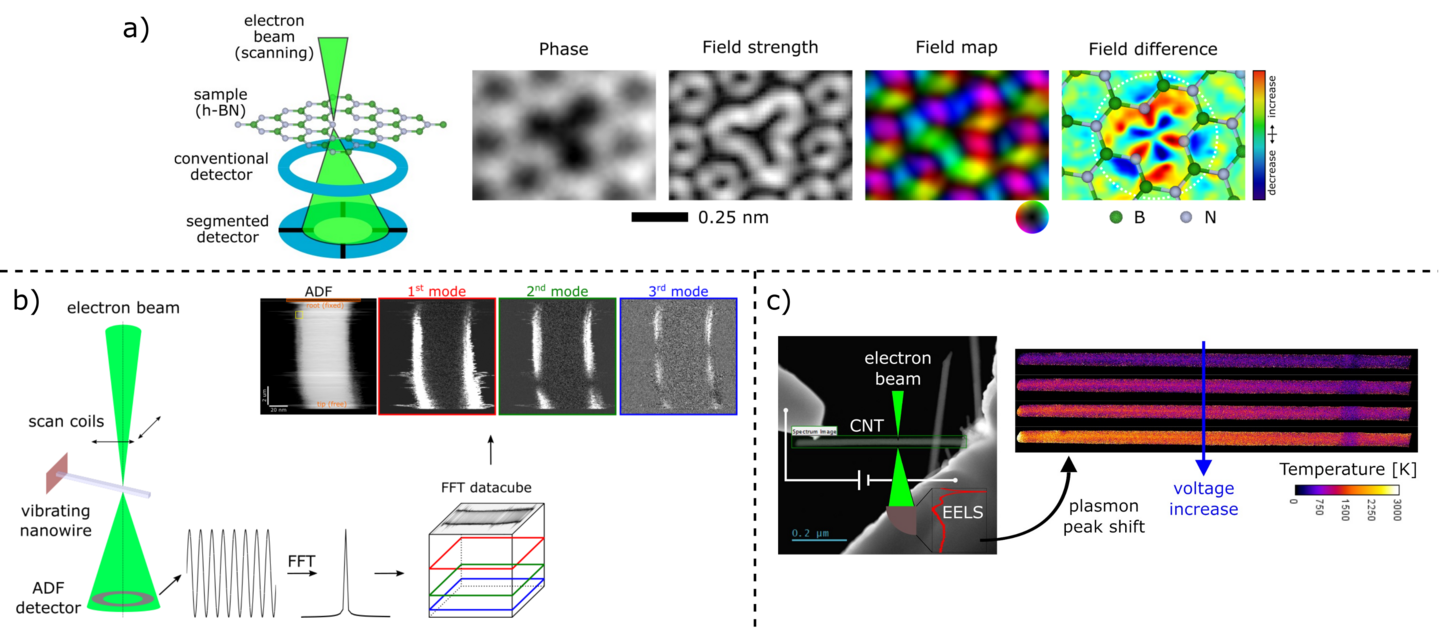
(figures reproduced from the four publications (DOIs: 10.1016/j.ultramic.2025.114292; 10.1021/acs.nanolett.2c03762; 10.1016/j.carbon.2022.10.006; 10.1021/acsnano.0c10849); © respective publishers)

➯ 1. Seeing faster: 100 MHz STEM

A major challenge in STEM is that scanning an electron probe across a specimen takes time. A programmable 100 MHz scan controller was developed to dramatically accelerate this process while minimizing distortions caused by the finite response of the microscope's scan coils. Using a spiral scanning strategy, high-quality images can be acquired in frames as short as 0.9 ms. The system also enables precise control of the electron dose, allowing the available dose to be used more efficiently and reducing unnecessary exposure. This combination of speed and dose control provides an important foundation for imaging dynamic and beam-sensitive materials.

➯ 2. Measuring nanoscale motion: frequency-selective imaging

Nanoscale resonators can vibrate at remarkably high frequencies, but directly observing their different modes of motion is challenging. By combining aberration-corrected STEM with broadband time-domain signal acquisition and Fourier analysis, this work turns the electron microscope into a tool for mapping mechanical vibrations in nanoscale resonators. The method successfully visualized the first six thermal vibration modes of a singly clamped nanowire, including higher-order modes with sub-ångström amplitudes that are difficult to distinguish using conventional imaging. The experimentally measured mode profiles agree with finite-element calculations, demonstrating how electron microscopy can provide direct, spatially resolved insight into the mechanical dynamics of nanoscale resonators.

➯ 3. Measuring heat: nanometer-scale thermometry

Temperature is particularly difficult to measure in nanoscale devices: conventional thermometers simply cannot be placed where the most interesting phenomena occur. Here, plasmon spectroscopy provides an elegant solution. When a carbon nanotube is electrically heated, its plasmon response changes with temperature. By measuring these changes with an electron beam, the temperature distribution along the nanotube can be determined with nanometer-scale spatial resolution. The technique effectively transforms the electron microscope into a highly localized thermometer, providing a direct view of heat generation and transport in nanoscale materials.

➯ 4. Making electric fields visible: atomic-scale DPC-STEM

Electric fields are fundamental to the behavior of materials, yet they are invisible in ordinary electron microscopy images. Differential phase contrast STEM provides a way to reveal them. By measuring tiny changes in the trajectory of the electron probe, the local electric field can be reconstructed while simultaneously recording the atomic structure. Applied to hexagonal boron nitride, the technique reveals enhanced electric fields around boron monovacancies and extended defects, linking the atomic structure of defects directly to their electromagnetic properties. Real-time field mapping further opens the possibility of following these effects as materials evolve.

Summary

From milliseconds to atomic dimensions, these techniques expand what can be seen and measured with an electron microscope. Faster scanning captures fleeting events while reducing electron exposure; frequency-selective imaging reveals nanoscale mechanical motion; plasmon spectroscopy turns nanoscale structures into thermometers; and differential phase contrast makes atomic-scale electric fields visible. Rather than treating electron microscopy as a technique for obtaining ever-sharper images, this research takes a broader approach: developing new ways to make the electron microscope interact with, measure, and ultimately understand materials. The result is a more versatile generation of electron microscopy techniques capable of connecting atomic structure with the dynamic, thermal, and electromagnetic properties that govern material function.

この機能は所内限定です。
この機能は所内限定です。

▲ Go to the top of this page