SAMURAI - NIMS Researchers Database

HOME > Profile > TSUKAGOSHI, Kazuhito

External affiliations

  • 国立陽明交通大学 電子物理系 Joint Appointment Professor
  • 国立中興大学 Physics Department Visiting Professor
  • 千葉工業大学 連携大学院客員教授

Research

Keywords

パイ電子系、ナノエレクトロニクス、電流注入

酸化膜半導体や2次元半導体で10nmスケールトランジスタの作製と電気伝導特性評価を進めています。

PublicationsNIMS affiliated publications since 2004.

Research papers
Books
Proceedings
Presentations
Misc

Society memberships

応用物理学会

Research Center for Materials Nanoarchitectonics (MANA)
Title

Nano-scale n-type and p-type transistors

Keywords

Oxide-semiconductor, 2D-semiconductor, Nano-scale fabrication, ALD, transistor, electrical characterization

Overview

Our research on thin-film transistors involves developing new materials and deposition methods tailored to specific applications, as well as nanoscale microfabrication techniques and evaluating electrical conductivity characteristics. We are developing n-type and p-type ultra-thin semiconductor films using sputtering, coating, and atomic layer deposition (ALD). Current challenges include exploring manufacturing methods that meet the upper limit of heating temperature and selecting electrode metals. In particular, to meet the demand for reduced process temperature, we are attempting to form semiconductor films by stacking atomic layers using ALD and controlling their properties through elemental doping.

Novelty and originality

・While conventional materials required a 400-600°C process, the application of proprietary new materials and oxidation methods has enabled the fabrication of inorganic thin-film transistors at temperatures below 200°C.
・Conductivity is controlled through ultra-thin film thinning and doping.
・Transistor structures are formed using semiconductor thin films (n-type, p-type) with a thickness of 1-5 nm.
・Analysis of conduction function and terminal current injection mechanism.
・Feedback is provided to the film deposition process based on the results of the conduction characteristic analysis.

Details

image

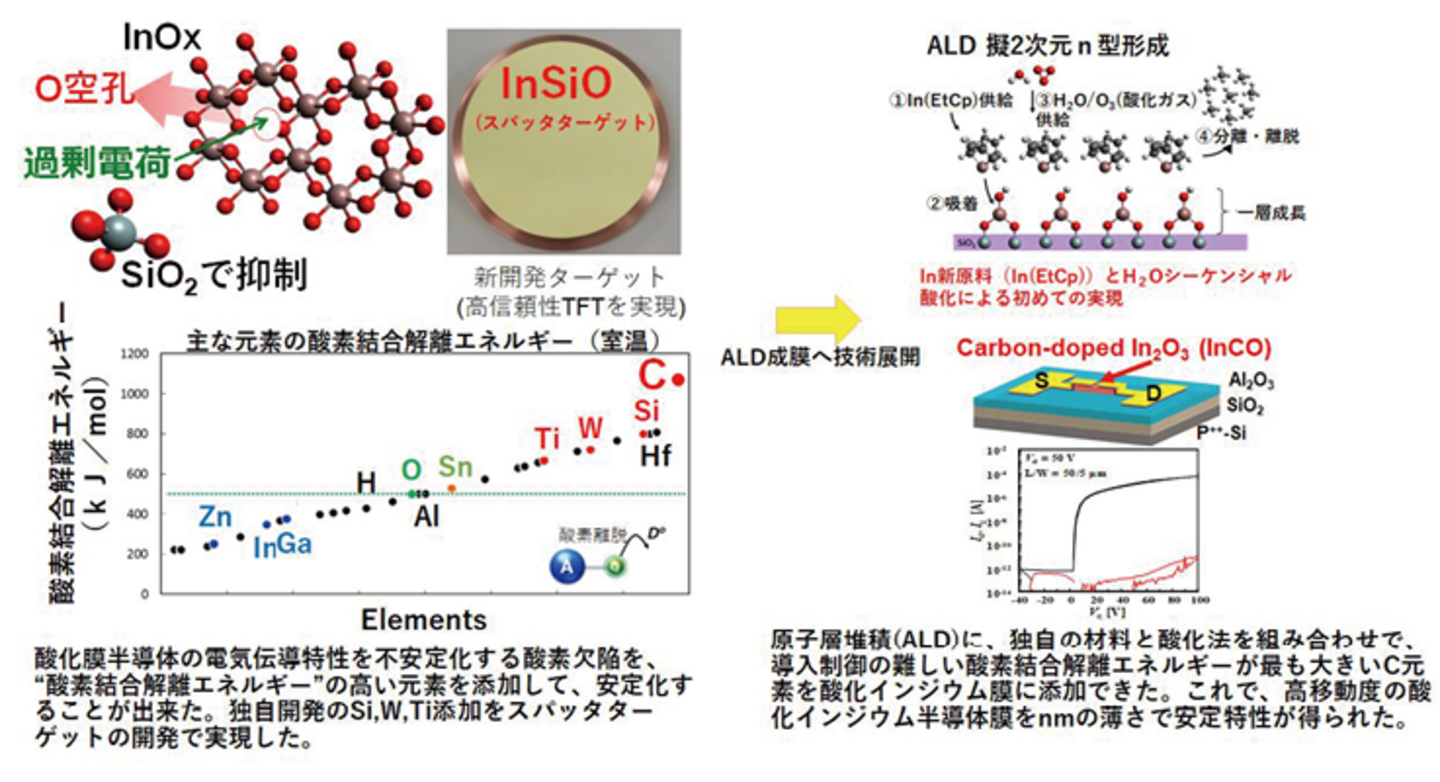
We identified that the instability (low reliability) in the electrical conductivity characteristics of oxide film transistors lies in the instability of oxygen vacancies, and found that this can be controlled by adding elements with high oxygen bond dissociation energy. Generally, material selection is made with an emphasis on ease of thin film fabrication and mobility, but this results in low reliability. Using indium oxide films, which inherently have high mobility, as a substrate, we significantly improved device reliability by adjusting the added elements and their amounts using sputter deposition. With ALD deposition, which enables low-temperature processes, we were able to control and retain carbon, which has a high oxygen bond dissociation energy, making it possible to create highly reliable transistors even with ultra-thin films of about 5 nm thickness. Furthermore, we use our own ALD precursor and have made unique improvements to the deposition structure. Reducing device resistance through electrode metal selection based on current injection mechanism analysis is also useful for improving reliability.

Summary

In addition to developing oxide film semiconductor materials and devices, we have also fabricated transistor structures using graphene and chalcogenide semiconductors and evaluated their electrical properties. We have also fabricated devices using polymorphic film fragments and nanowires. Currently, we are attempting to control the properties of ultrathin films with an oxide film thickness of 1-5 nm, and are exploring atomic-scale control of ultrathin n-type and p-type films.

この機能は所内限定です。
この機能は所内限定です。

▲ Go to the top of this page