HOME > Profile > WAKAYAMA, Yutaka
- Address
- 305-0044 1-1 Namiki Tsukuba Ibaraki JAPAN [Access]
Accepting Students
External affiliations
- 東京電機大学 客員教授
- 大阪大学 招聘教授
Research
- Keywords
単一電子素子、機能性有機トランジスタ、分子ナノ構造制御
PublicationsNIMS affiliated publications since 2004.
Research papers
- Ryoma Hayakawa, Yuho Yamamoto, Kosuke Yoshikawa, Yoichi Yamada, Yutaka Wakayama. Reconfigurable artificial synapses with an organic antiambipolar transistor for brain-inspired computing. Journal of Materials Chemistry C. (2025) 14234-14241 10.1039/d5tc01712b Open Access
- S. Fatemeh Mousavi, Aisha Ahsan, Aaron Oechsle, Narmadha Devi, Yoshitaka Matsushita, Luiza Buimaga-Iarinca, Cristian Morari, Waka Nakanishi, Katsuhiko Ariga, Yutaka Wakayama, Yusuke Yamauchi, Thomas A. Jung, Jonathan P. Hill. Emergence of conformational diversity and complexity of supramolecular structure by the interaction of a simple molecule with a uniform surface. Communications Chemistry. 8 [1] (2025) 214 10.1038/s42004-025-01607-x Open Access
- 早川 竜馬, パニグラヒ デブダッタ, 若山 裕. 有機アンチ・アンバイポーラトランジスタを用いた多機能論理回路. Accounts of Materials & Surface Research. 9 [1] (2024) 1-10 Open Access
Books
- HAYAKAWA, Ryoma, CHIKYO, Toyohiro, WAKAYAMA, Yutaka. Quantum Molecular Devices Toward Large-Scale Integration. NIMS Monographs: System-Materials Nanoarchitectonics. Springer Nature, 2022, 15.
- WAKAYAMA, Yutaka, ARIGA, Katsuhiko. System-Materials Nanoarchitectonics. System-Materials Nanoarchitectonics. Springer, 2022, 338.
Proceedings
- MITSUI, Tadashi, WAKAYAMA, Yutaka, ONODERA Tsunenobu, HAYASHI Takeru, IKEDA, Naoki, SUGIMOTO, Yoshimasa, TAKAMASU, Tadashi, OIKAWA Hidetoshi. Light Splitting Function of Branched Chains of Transparent Microspheres. Proceedings of ICTON 2010. (2010) Tu.B4.4-1-Tu.B4.4-4
- Jonathan P. Hill, Yutaka Wakayama, Misaho Akada, Katsuhiko Ariga. Two-dimensional molecular array of porphyrin derivatives with bright and dark spots as a model of two-digit molecular-dot memory. SYNTHETIC METALS. (2009) 765-768 10.1016/j.synthmet.2008.12.016
- ARIGA, Katsuhiko, HILL, Jonathan, WAKAYAMA, Yutaka. Supramolecular chemistry in two dimensions:self-assembly and dynamic function. PHYSICA STATUS SOLIDI A-APPLICATIONS AND MATERIALS SCIENCE. (2008) 1249-1257
Presentations
- 宇澤 拳太郎, 早川 竜馬, 岩崎 拓哉, 渡邊 賢司, 谷口 尚, 若山 裕, 森山 悟士. 新規ロジックデバイス応⽤に向けた⼆次元材料アンチ・アンバイポーラトランジスタの作製と 電気伝導特性評価. 第2回応用物理学会 関東地区 学生研究交流会. 2026
- BERA, Jayanta, HAYAKAWA, Ryoma, WAKAYAMA, Yutaka. Organic Antiambipolar Transistor for Low-Voltage Quaternary Logic Inverter. 12th International Conference on Molecular Electronics and Bioelectronics (M&BE 12). 2026
- 奥 伊吹, 和泉 龍成, 合田 智実, HAYAKAWA, Ryoma, 磯部 桃花, 大貫 良輔, WAKAYAMA, Yutaka, 吉岡 伸也, 金井 要. Optoelectronic synaptic device using poly (heptazine imide). M&BE12 (12th International Conference on Molecular Electronics and Bioelectronics). 2026
Misc
- 早川 竜馬, 知京 豊裕, 若山 裕. 機能性分子を量子ドットに用いた共鳴トンネルデバイス. Molecular Electronics and Bioelectronics 応用物理学会 有機分子・バイオエレクトロニクス分科会 会誌. (2018) 68-71
- 中払 周, マッカージー バブル, 若山 裕. 二次元層状物質を使った光多値メモリの開発. 月刊 機能材料. (2021) 58-64
- 廣芝 伸哉, 早川 竜馬, 若山 裕. On-terraceグラフォエピタキシによるC8-BTBTナノワイヤの異方成長制御. 応用物理学会有機分子・バイオエレクトロニクス分科会会誌. (2020) 109-114
Published patent applications
Society memberships
応用物理学会, Materials Research Society, European Materials Research Society
Awards
- 優秀論文賞(MNC2018) (2019)
- 応用物理学会解説論文賞 (2017)
- Best Poster Award (MRS Spring meeting 2010) (2010)
- 応用物理学会講演奨励賞 (1997)
Funds
- 二次元ヘテロ界面の精密設計による革新的演算デバイスの開拓 (2024)
- 有機へテロ界面で制御する特異な電気伝導と革新的演算素子への応用 (2023)
- 次世代有機エレクトロニクスを拓く革新的演算機構 (2023)
- 光で制御する有機多値論理演算デバイスの開発 (2021)
- 集積度の飛躍的な向上を目指した有機負性抵抗トランジスタの開発 (2019)
- トランジスタ型超高感度イオンセンサーの開発とセシウムイオン検出への応用 (2016)
- 分子超格子を使った分子トンネル素子の開発 (2016)
- 分子で創る完全へテロ界面と新規分子デバイスへの応用 (2016)
- フォトクロミックエレクトロニクスに向けた光異性化分子の集積化と光電変換機能 (2015)
- 分子で創る超格子: 分子へテロ界面形成過程の直接観察からのアプローチ (2014)
- 分子ナノワイヤーを用いた多値論理デバイスの開発 (2012)
- 異種分子組織膜のメモリ機能への応用:シリコンプロセスとの融合を探る (2011)
- ナノワイヤアレイの創製とデバイス応用 (2009)
Research Center for Materials Nanoarchitectonics (MANA)
Nanomaterials arcnitectonics for novel nanoelectronicws
Thin film transistor, heterointerface, multi-value logics, logic gate circuits, logic-in-memory
Overview
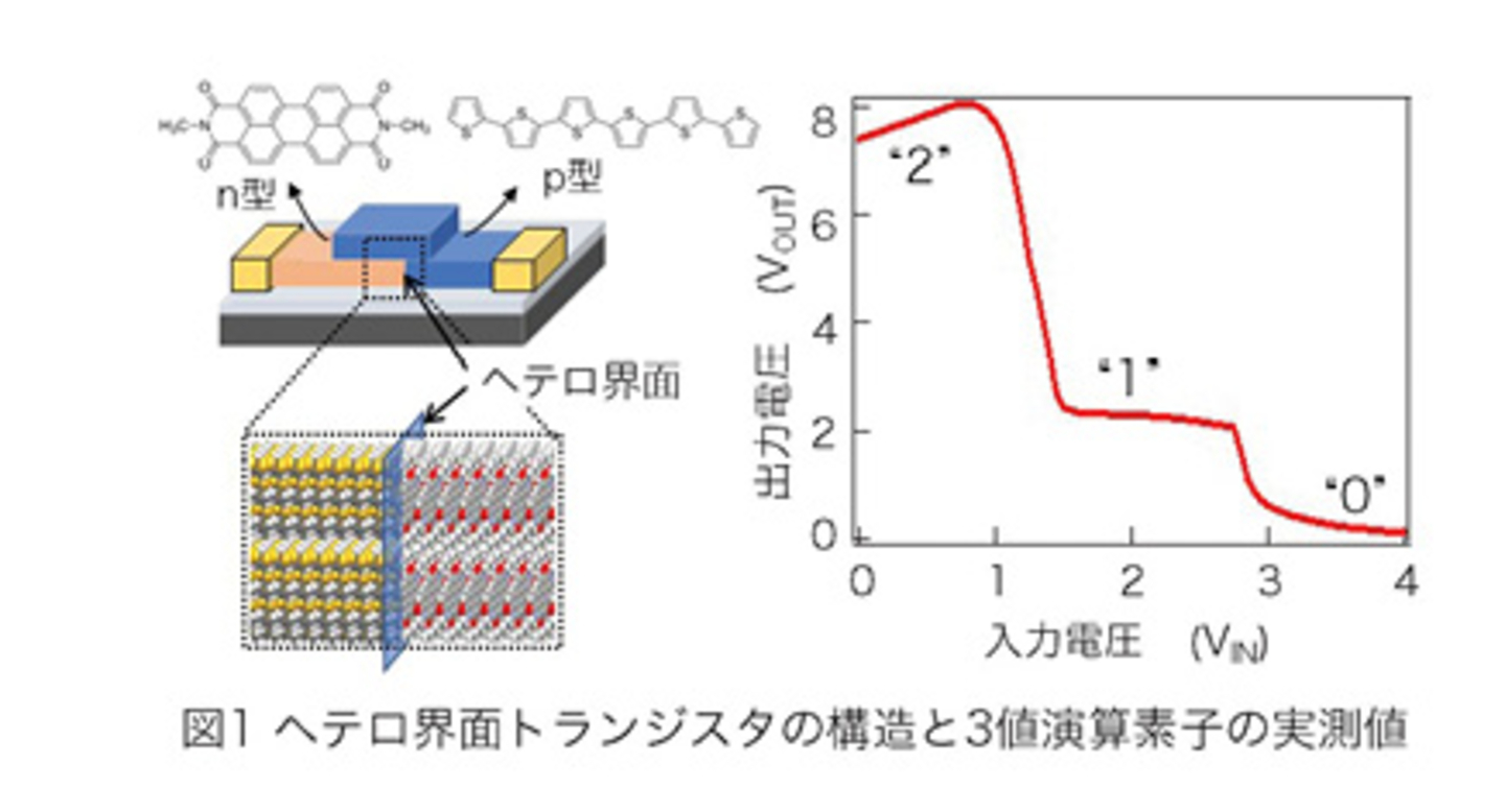
To pioneer a new field in next-generation nanoelectronics, we will realize a novel computing mechanism that goes beyond conventional binary (0,1) arithmetic and CMOS-based circuit designs by fully utilizing our independently developed heterointerface transistors. A pn heterointerface is formed in the center of this transistor, exhibiting a unique characteristic where the drain current sharply increases and decreases. Focusing on this negative-resistance-like phenomenon, we have successfully demonstrated a ternary computing device representing three operational values (0, 1, 2). Building upon these achievements, we will establish the operating principles for a new group of devices, including multi-value arithmetic of four or more values, reconfigurable logic devices, logic-in-memory integrating processing and storage, and neuromorphic elements with memory controlled by pulse signals.
Novelty and originality
Operating principle of a novel transistor aiming at non-von Neumann computing architectures.
Specific current control through precise design of heteromaterial interfaces in transistors.
Development of new electronic devices to overcome the limitation of integration density, growing power consumption and data processing speed.
Details
Development of multi-valued logic devices: As shown in Figure 1, a pn heterointerface is formed at the center of this transistor, exhibiting a unique characteristic where the drain current sharply increases and decreases. By utilizing negative differential resistance—where current decreases as voltage increases—we successfully demonstrated a ternary logic device representing three operational values (0, 1, 2). Compared with conventional binary logic (0, 1) elements, ternary logic allows drastic increase in integration density. Furthermore, quaternary logic devices with four operational values (0, 1, 2, 3) have recently been realized.
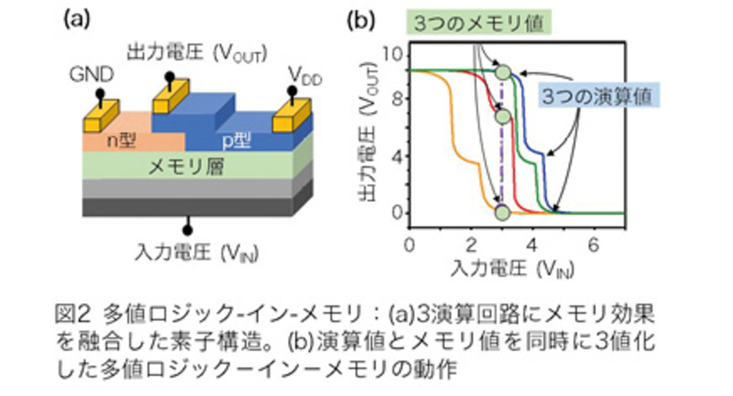
Development of multi-valued logic-in-memory: As shown in Fig. 2, we demonstrated the operation of a multi-valued logic-in-memory device in which the two functions of computation and memory are operated by a single element, and both functions are multi-valued simultaneously. While the separation of computation and storage in conventional von Neumann architecture devices poses a bottleneck for device functionality, this achievement goes beyond merely solving that issue. By successfully multi-valuing both computation and memory simultaneously, this result leads to a dramatic improvement in integration density and recording density, as well as the suppression of power consumption.
Summary
While nanoelectronic devices are actively developed as next-generation AI components, challenges like integration limits and rising power consumption persist. To solve these, this study proposes novel device structures, materials, and operating principles.