HOME > Profile > NABATAME, Toshihide
- Senior Scientist with Special Missions, Research Center for Materials Nanoarchitectonics (MANA)
- NIMS Invited Researcher, Thin Film Electronics Group, Quantum Materials Field, Research Center for Materials Nanoarchitectonics (MANA)
- NIMS Invited Researcher, LSTC Semiconductor Materials Research Lab, External Collaboration Division
- Address
- 305-0044 1-1 Namiki Tsukuba Ibaraki JAPAN [Access]
Research
- Keywords
半導体CMOS、電子デバイス、ナノ薄膜形成技術、材料物性評価
PublicationsNIMS affiliated publications since 2004.
Society memberships
応用物理学会, Institute of Electrical and Electronics Engineers
Research Center for Materials Nanoarchitectonics (MANA)
原子層堆積法による新ナノ薄膜・半導体デバイス
原子層堆積法,ナノラミネート,HfO系強誘電体膜,InO系酸化物半導体膜,HfO系アモルファス絶縁膜,ZrO2低温度結晶成長,SiO2選択成長
Overview
半導体デバイスは、3次元構造で、絶縁膜及び電極共にナノメーターの膜厚で作製されています。原子層堆積法(ALD)は、飽和表面吸着反応の特徴を有しており、3次元構造のホール内壁にも均質な膜を形成できます。半導体デバイスとして、DRAM、強誘電体デバイス、GaNパワーデバイス及び酸化物半導体トランジスタがあり、各々で、期待されている材料、膜厚及び構造が異なります。このニーズに答えるように、幅広い材料探索、ALD原料の選択、ALD成膜条件を、作製したデバイスの電気特性をフィードバックさせて、研究を進めています。
Novelty and originality
ALDメカニズムの新提案及びユニークなアイデアによるALD作製技術で、下記を達成しました。
● ALDによるSiO2膜成長が、下地基板の酸素の電気陰性度で決まるメカニズムを初めて見出した。
● 新規Hf/Zrカクテル原料を用いる事で、HfZrO系強誘電体薄膜の300℃低温度形成に成功した。
● 高誘電率でアモルファスなHfSiO及びHfAlO絶縁膜を、GaNパワーデバイスの絶縁膜として提案した。
Details
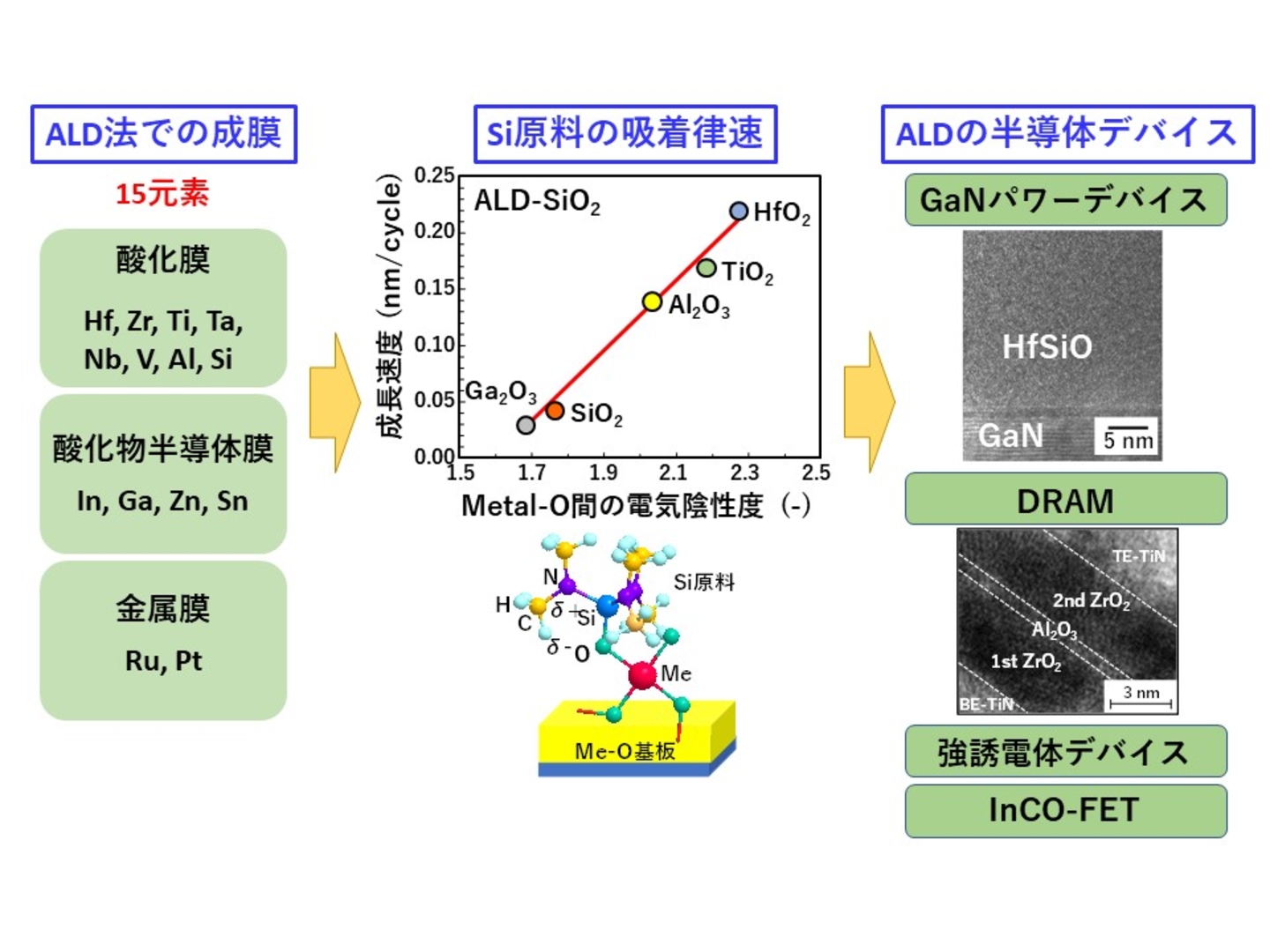
酸化膜として8元素、酸化物半導体膜として4元素及び金属膜として2元素のALD成膜を実施した20年以上に亘るデータの蓄積を基に、半導体デバイスの要求に対応しています。その中で、Si原料を用いたALD成膜で、ALD成長でSi原料の正電荷のSi原子が下地基板の負電荷の酸素に吸着しますが、この吸着が下地基板のMetal-Oの電気陰性度の差で決定されることを初めて見出しました。これは、下地材料を変えることでSiO2膜の選択成長ができる事を示しています。この様にALDメカニズムを理解して、GaNパワーデバイスではアモルファスなHfSiO膜、DRAMではZrO2/Al2O3/ZrO2スタック構造膜を形成しています。
Summary
ALD法は、既に、半導体デバイスの量産プロセスにも使われており、研究レベルで得られたALDデータが、そのまま技術移管がスムーズに進むメリットがあります。