
- Left
- No longer at NIMS since October 2023
Research
- Keywords
nanomaterials; nanoelectronics; carbon nanotube; 2D materials; chemical vapor deposition; transistors
PublicationsNIMS affiliated publications since 2004.
Society memberships
Japanese Society of Applied Physics, The Chemical Society of Japan
Awards
- Excellent Poster Presentation Award of MANA INTERNATIONAL SYMPOSIUM jointly with ICYS (2019)
- 日本化学会 第99春季年会 優秀講演賞(学術) (2019)
Funds
- 日本学術振興会(JSPS) 基盤研究(C) (2021)
- 日本学術振興会(JSPS) 若手研究 (2019)
Research Center for Materials Nanoarchitectonics (MANA)
Wafer-scale 2D semiconductors for flexible inkjet-printed electronics
Two-Dimensional Semiconductors, Chemical Vapor Deposition, Integration, Transistors
Overview
The advancement of smart society heavily depends on the use of flexible and wearable electronic devices. Among various semiconductor materials, two-dimensional (2D) semiconductors such as transition metal dichalcogenides (TMDs) (MX2, M=Mo, W; X=S, Se, Te) offer great promise. These TMDs possess atomic thinness, mechanical flexibility, durability, excellent electrical and optical properties, as well as chemical stability, making them superior to rigid 3D semiconductors. Consequently, it is crucial to develop innovative techniques for growing 2D TMD films and integrating them into flexible devices. To address this need, we have successfully developed a straightforward and replicable chemical vapor deposition (CVD) method for synthesizing 2D TMDs with large dimensions and exceptional electrical and optical qualities.
Novelty and originality
• Wafer-scale and patterned 2D TMDs are grown using an innovative CVD technique that utilizes molten salts as precursors.
• Effective n-type and p-type doping of 2D TMDs is accomplished by employing mixed molten-salt precursors.
• High-efficiency and cost-effective integration of 2D TMD-based thin-film transistors (TFTs) with inkjet printing technique.
Details
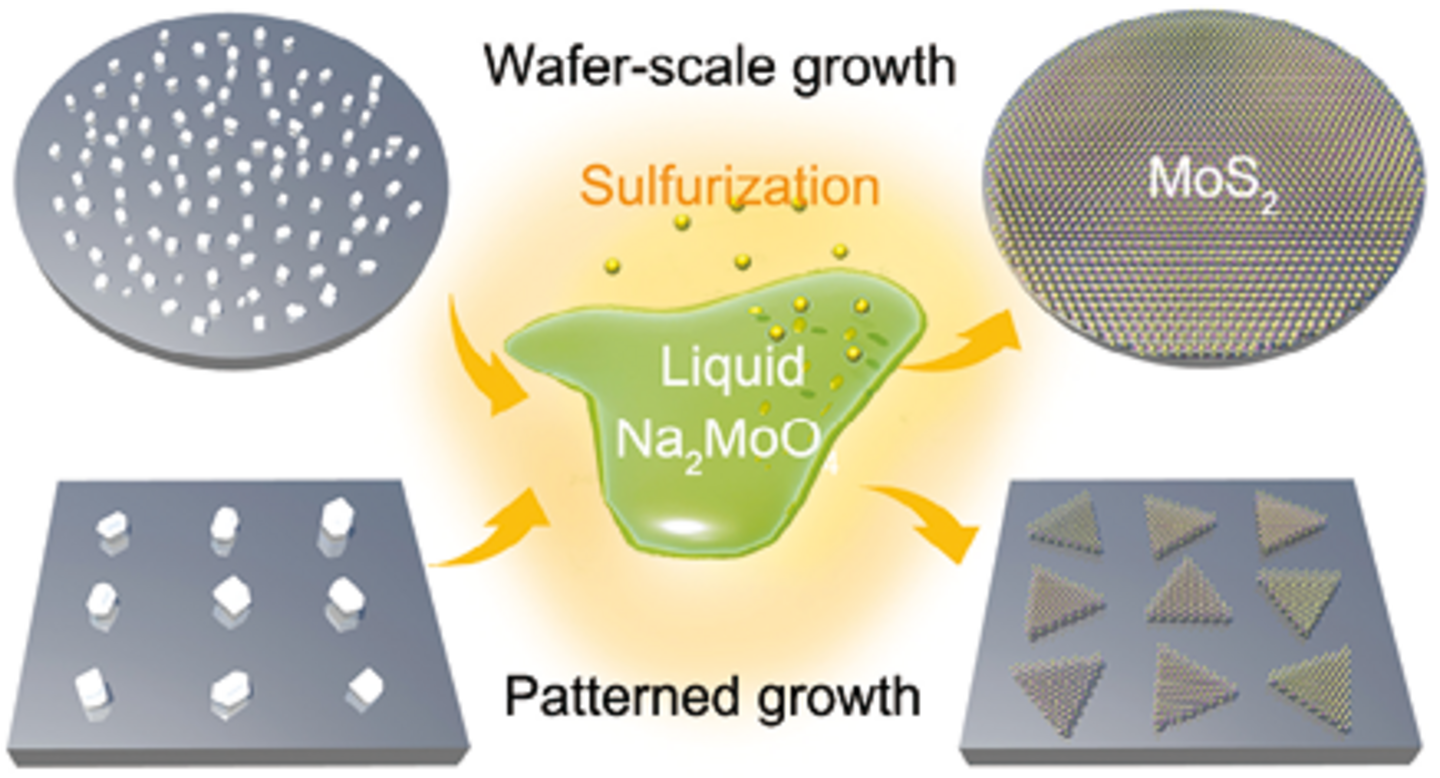
Schematic illustration of the deposition of molten salt, Na2MoO4 for CVD growth of wafer-scale and patterned MoS2 film. In general, 2D TMDs (MX2, M=Mo, W; X=S, Se, Te) can be grown with molten salts, e.g., Na2MoO4, Na2WO4, NaReO4 and NaVO3.
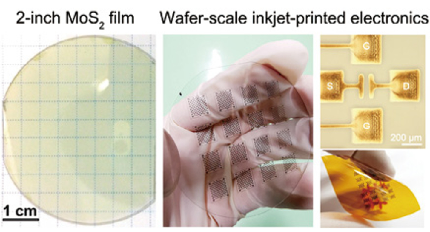
The photographs showcase a 2-inch wafer-scale MoS2 film, inkjet-printed TFTs on sapphire substrates, and flexible MoS2-based TFTs on a polyimide film. Further endeavors will be dedicated to the exploration of 2D TMD-based electronic devices, aimed at sensing and detecting various physical and chemical signals. These efforts will play a crucial role in advancing the development of 2D TMD-based flexible and wearable devices.
Summary
Molten-salt CVD technique is employed to synthesize wafer-scale and patterned 2D TMDs. These remarkable materials exhibit excellent mobility and display a high current on/off ratio when utilized as channel components in TFTs. In the future, considerable focus will be directed towards integrating 2D TMDs into flexible and wearable sensors and detectors using the inkjet printing technique.